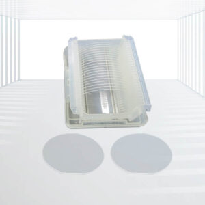
陶瓷基板1.jpg "Kingwim Optics Thick Flim Metalized Beryllium Oxide Ceramic Substrates")
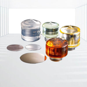
陶瓷基板2.jpg "Kingwim Optics Thick Flim Metalized Beryllium Oxide Ceramic Substrates")
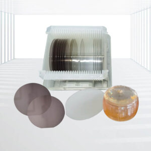
陶瓷基板3.jpg "Kingwim Optics Thick Flim Metalized Beryllium Oxide Ceramic Substrates")
Thick Flim Metalized Beryllium Oxide Ceramic Substrates
High Ruggedness: Robust construction minimizes the possibility of outgassing.
Nickel Plating: Ensures durability without blistering.
Versatility: Suitable for various applications requiring high thermal and electrical performance.
Applications: Wire Bonding Platforms, Microwave PCBs, Thermoelectric Coolers (TEC) for Lasers, Hybrid Integrated Circuits (HIC) for Automotive, High-Power Semiconductor Modules, Hermetic Electrical Packaging, etc.
Thick Film Metalized Ceramic Substrates involve screening ceramics with conductor, resistor, and resistor metal pastes, followed by firing. This technique is engineered to achieve specific functionalities, offering significant advantages over thin film metallization in terms of high-volume production efficiency and suitability for circuits with less stringent precision requirements.
Beryllium Oxide (Beryllia/BeO) ceramics are renowned for their exceptional thermal conductivity, making them ideal for applications requiring efficient heat dissipation.
Kingwin Optics provides Thick Film Metalized BeO Ceramic Substrates, leveraging thick-film WMn/MoMn metallization with nickel electroplating. This process ensures substrates with outstanding bonding strength, weldability, and tensile strength exceeding 20MPA.
Specifications:
| Parameters/Models | BEO99 | BEO99.5 | |
| Volume Density | ≥2.85g/cm3 | ≥2.88g/cm3 | |
| Flexural Strength | ≥200Mpa | ≥200Mpa | |
| Average Coefficient of Expansion (at 25-500°C) | 7.0-8.0×10⁻⁶/K | 7.0-8.0×10⁻⁶/K | |
| Thermal Conductivity | at 25°C | ≥260W/m.K | ≥285W/m.K |
| at 100°C | ≥190W/m.K | 200W/m.K | |
| Dielectric Constants | at 1MHz | 6.7±0.2 | |
| at 10GHz | 6.9±0.2 | 6.8±0.2 | |
| Dielectric Loss Tangent | at 1MHz | ≤4×10⁻⁴ | ≤4×10⁻⁴ |
| at 10±0.5GHz | ≤6×10⁻⁴ | ≤4×10⁻⁴ | |
| Volume Resistivity | ≥1014 Ω.cm (at 20 °C) | ≥1014 Ω.cm (at 100 °C) | |
| Puncture Strength | ≥30kV/mm | ≥40kV/mm | |
| Thermal Shock Resistance | Excellent | Excellent | |
| Chemical Stability | 1:9 HCL | ≤0.1mg/cm2 | ≤0.1mg/cm2 |
| 10% NaOH | ≤0.1mg/cm2 | ≤0.1mg/cm2 | |
| Air Tightness | ≤5×10-12Pa.m3/s | ≤5×10-12Pa.m3/s | |
| Average Grain Size | 10-20μm | 10-20μm | |
Manufacturing Process:
1.Thick Film Treatment:
- Materials: Tungsten (W) and Manganese (Mn), or Molybdenum (Mo) and Manganese (Mn).
- Process: Metal pastes are printed on bare BeO ceramics using silk-screen techniques and fired at high temperatures above 800℃.
2.Nickel Electroplating:
- Ensures high bonding force and excellent tensile strength.
- Prevents blistering, enhancing durability and reliability.
3.Pattern Distribution:
- Metal films can cover entire surfaces or be distributed in precise circuit patterns.
- Dimensional tolerances of circuit patterns are maintained within 0.02mm.
4.High-Precision Laser Processing:
- Includes laser-cutting, laser-drilling, and laser-marking.
- Ensures tight geometric monitoring and high precision.
Features:
- High Ruggedness: Robust construction minimizes the possibility of outgassing.
- Nickel Plating: Ensures durability without blistering.
- Versatility: Suitable for various applications requiring high thermal and electrical performance.
Applications:
- Wire Bonding Platforms: Ideal for creating reliable wire bonds.
- Microwave PCBs: Excellent preforms for microwave printed circuit boards.
- Thermoelectric Coolers (TEC) for Lasers: Efficient heat dissipation for laser applications.
- Hybrid Integrated Circuits (HIC) for Automotive: Reliable performance in automotive electronics.
- High-Power Semiconductor Modules: Supports high-power electronic applications.
- Hermetic Electrical Packaging: Ensures airtight electrical packaging for sensitive components.
For detailed specifications, custom shapes, and additional information on Thick Film Metalized BeO Ceramic Substrates, reach out to Kingwin Optics. Our advanced manufacturing capabilities ensure high-quality, reliable solutions tailored to your specific needs.