 Crystals and Wafers")
 Crystals and Wafers")
 Crystals and Wafers")
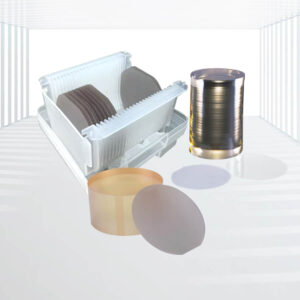
Silicon (Si) Crystals and Wafers
High-Purity Polycrystalline Silicon Ingots:Silicon wafers are made from high-purity polycrystalline silicon ingots, ensuring minimal impurities and consistent material properties.
Controlled Manufacturing Process:The manufacturing process follows a controlled and organized sequence, including crystal growth, slicing, chamfering/grinding (lapping), surface etching/polishing, cleaning, inspection, packaging, and other processes, ensuring high-quality wafers.
Customizable Doping:Doping with designed concentrations can be introduced into the silicon crystal lattice to alter its electrical properties and create regions with specific conductivity (n-type or p-type) required for semiconductor devices.
Versatile Platform for Thin Film Deposition:Si wafers serve as excellent platforms for the deposition of various thin films to achieve specific functions, making them versatile for a wide range of applications.
Multiple Applications:Kingwin Optics’ Silicon (Si) wafers and substrates are used as substrates for GaN (Gallium Nitride) epitaxial film growth, semiconductors, and solar cells, demonstrating their versatility and wide range of applications.
Applications: GaN Epitaxial Film Growth, Semiconductors, Solar Cells, etc.
Silicon (Si) wafers are a fundamental component in the semiconductor industry, serving as the basis for a wide range of electronic devices. Kingwin Optics offers various grades of Silicon (Si) wafers and substrates, manufactured using controlled and organized processes that ensure high quality and consistency. These wafers are used as substrates for GaN (Gallium Nitride) epitaxial film growth, semiconductors, and solar cells.
Specifications:
| Crystal Structure | M3 | Melt Point(℃) | 1420 |
| Density(g/cm3) | 2.4 | ||
| Doping Material | No | b-doped | p-doped |
| Type | Ⅰ | P | N |
| Resistivity | >1000Ωcm | 10-3~104Ωcm | 10-3~104Ωcm |
| EPD | ≤100∕cm2 | ≤100∕cm2 | ≤100∕cm2 |
| O Content (/cm3) | ≤1~1.8×10¹⁸ | ≤1~1.8×10¹⁸ | ≤1~1.8×10¹⁸ |
| C Content (/cm3) | ≤5×10¹⁶ | ≤5×10¹⁶ | ≤5×10¹⁶ |
Key Advantages:
- High-Purity Polycrystalline Silicon Ingots:Silicon wafers are made from high-purity polycrystalline silicon ingots, ensuring minimal impurities and consistent material properties.
- Controlled Manufacturing Process:The manufacturing process follows a controlled and organized sequence, including crystal growth, slicing, chamfering/grinding (lapping), surface etching/polishing, cleaning, inspection, packaging, and other processes, ensuring high-quality wafers.
- Customizable Doping:Doping with designed concentrations can be introduced into the silicon crystal lattice to alter its electrical properties and create regions with specific conductivity (n-type or p-type) required for semiconductor devices.
- Versatile Platform for Thin Film Deposition:Si wafers serve as excellent platforms for the deposition of various thin films to achieve specific functions, making them versatile for a wide range of applications.
- Multiple Applications:Kingwin Optics’ Silicon (Si) wafers and substrates are used as substrates for GaN (Gallium Nitride) epitaxial film growth, semiconductors, and solar cells, demonstrating their versatility and wide range of applications.
Applications:
- GaN Epitaxial Film Growth:Silicon wafers serve as substrates for the growth of GaN epitaxial films, enabling the production of high-quality GaN-based devices.
- Semiconductors:Silicon wafers are essential for the production of semiconductors, serving as the foundation for various electronic devices.
- Solar Cells:Silicon wafers are used in the production of solar cells, leveraging their ability to convert sunlight into electricity.
Kingwin Optics offers various grades of Silicon (Si) wafers and substrates, manufactured using controlled and organized processes to ensure high quality and consistency. These wafers are used as substrates for GaN epitaxial film growth, semiconductors, and solar cells, demonstrating their versatility and wide range of applications. With customizable doping and excellent thin film deposition properties, Kingwin Optics’ Silicon (Si) wafers and substrates provide tailored solutions for diverse research and industrial applications.

")
晶体和晶圆1-300x300.jpg)
晶体和晶圆2-300x300.jpg "Kingwim Optics SAW Quartz (SiO2) Crystals and Wafers")
3-300x300.jpg "Kingwim Optics SrLaAlO4 (Strontium Lanthanum Aluminate) Crystal Wafers")