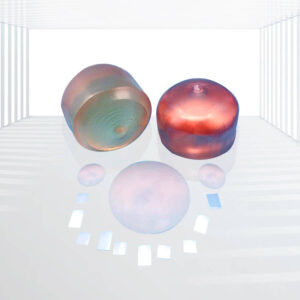
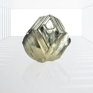
 Crystals and Wafers")
 Crystals and Wafers")
 Crystals and Wafers")
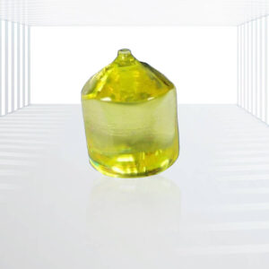
Silicon Carbide (SiC) Crystals and Wafers
Exceptional Thermal Conduction: SiC has exceptional thermal conductivity, allowing for efficient heat dissipation in high-power devices. This results in reduced cooling necessities and improved device reliability.
Superior Mechanical Resilience: With high hardness and lightweight nature, SiC wafers are robust and durable, making them ideal for harsh operating conditions.
Broad Bandgap: The broad bandgap of SiC enables the production of devices with higher breakdown voltages and lower leakage currents, essential for high-voltage applications.
Large Electric Field Breakdown Strength: SiC’s ability to withstand large electric fields allows for the development of compact, high-efficiency power devices.
High-Temperature Endurance: SiC’s endurance to withstand high temperatures makes it suitable for applications where traditional silicon devices would fail.
Improved Switching Speeds: SiC-based power devices boast swifter switching speeds, leading to increased efficiency and reduced power loss.
Applications: High-Frequency Power Electronic Devices, RF Transistors, Optoelectronic Devices, Extreme Environmental Applications, etc.
Silicon Carbide (SiC) is a semiconductor material composed of silicon and carbon, renowned for its remarkable thermal conduction, superior mechanical resilience, broad bandgap, and large electric field breakdown strength. These unique properties make SiC an attractive material for high-power, high-frequency electronic components. Kingwin Optics offers custom SiC crystal wafers tailored to meet the demands of various applications, particularly in extreme environments.
Specifications:
| Main performance parameters | |
| Growth method | Seed crystal sublimation method, PVT (Physical Vapor Phase Transfer). |
| Crystal structure | hexagonal |
| Lattice constant | a=3.08 Å c=15.08 Å |
| density | 3.21 g/cm3 |
| direction | Growth axis or <0001> 3.5º |
| Band gap | 3.26 eV (Indirect) |
| hardness | 9.2(mohs) |
| Thermal conduction @300K | 5 W/ cm.k |
| Dielectric constant | e(11)=e(22)=9.66 e(33)=10.33 |
| size | 10×3,10×5,10×10,15×15,,20×15,20×20, |
| Dia2″,Di3″,Dia4″ | |
| thickness | 0.35mm, |
| polished | Single-sided or double-sided |
| Crystal orientation | <0001>±0.5º |
| Plane orientation accuracy: | ±0.5° |
| Edge Orientation Accuracy: | 2° (up to 1° for special requirements) |
| Beveled wafers | Wafers with edge-oriented crystal planes inclined at specific angles (1°-45°) can be processed according to specific needs |
| Ra: | ≤5Å(5µm×5µm) |
| wrap | Class 100 clean bag, Class 1000 clean room |
Advantages:
- Exceptional Thermal Conduction: SiC has exceptional thermal conductivity, allowing for efficient heat dissipation in high-power devices. This results in reduced cooling necessities and improved device reliability.
- Superior Mechanical Resilience: With high hardness and lightweight nature, SiC wafers are robust and durable, making them ideal for harsh operating conditions.
- Broad Bandgap: The broad bandgap of SiC enables the production of devices with higher breakdown voltages and lower leakage currents, essential for high-voltage applications.
- Large Electric Field Breakdown Strength: SiC’s ability to withstand large electric fields allows for the development of compact, high-efficiency power devices.
- High-Temperature Endurance: SiC’s endurance to withstand high temperatures makes it suitable for applications where traditional silicon devices would fail.
- Improved Switching Speeds: SiC-based power devices boast swifter switching speeds, leading to increased efficiency and reduced power loss.
Applications:
- High-Frequency Power Electronic Devices: SiC is widely used in the production of Schottky diodes, MOSFETs, JFETs, BJTs, PIN diodes, and IGBTs. These devices are critical components in power conversion systems, such as inverters and converters, used in renewable energy, electric vehicles, and industrial automation.
- RF Transistors: SiC’s high electron mobility and high saturation velocity make it an excellent material for RF transistors, enabling high-frequency operation with low noise and distortion.
- Optoelectronic Devices: SiC is applied as a backing material for blue LEDs, taking advantage of its excellent thermal and mechanical properties. It also has potential applications in UV LEDs and photodetectors.
- Extreme Environmental Applications: Kingwin Optics’ custom SiC crystal wafers are particularly suited for applications in aerospace, military industry, and nuclear energy, where high performance and reliability under extreme conditions are crucial.
Kingwin Optics specializes in offering custom SiC crystal wafers tailored to meet specific application requirements. These wafers offer optimum results in LED solid-state lighting and high-frequency devices, providing customers with high-quality, reliable products. Kingwin Optics’ wafers are manufactured using advanced processes to ensure consistent quality and performance, making them an excellent choice for demanding applications.
In summary, Silicon Carbide (SiC) crystals and wafers from Kingwin Optics combine exceptional properties with customizability, making them ideal for a wide range of high-performance, high-reliability applications.

1-300x300.jpg "Kingwim Optics LaAlO3 Substrates")
晶体和晶圆1-300x300.jpg)
晶体和晶圆2-300x300.jpg "Kingwim Optics SAW Quartz (SiO2) Crystals and Wafers")
 Crystals and Substrates")