Crystal and Substrates")
晶体及基片1.jpg "Kingwim Optics Zinc oxide (ZnO) Crystal and Substrates")
晶体及基片2.jpg "Kingwim Optics Zinc oxide (ZnO) Crystal and Substrates")
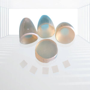
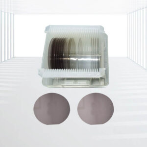
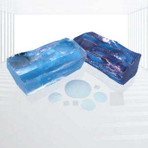
Zinc oxide (ZnO) Crystal and Substrates
Wide Bandgap: With a bandgap of 3.4 eV, ZnO is suitable for manifold blue and violet optoelectronic applications as well as UV devices.
Competitive Edge: The availability of large-size ZnO crystals offers a competitive advantage over other materials like GaN.
Optimal GaN Film Growth: ZnO substrates have a wurtzite structure with lattice constants well-matched to GaN, resulting in minimal lattice mismatch and optimal film growth.
Lattice Stress Absorption: ZnO is a soft compliant material that effectively absorbs lattice stress, protecting the growing GaN thin film.
Customized Solutions: Kingwin Optics offers customized high-quality ZnO crystal substrates and wafers to meet specific application requirements.
Applications: Optoelectronic Devices, UV Devices, Thin Film Growth, Research and Development, etc.
Zinc Oxide (ZnO) crystal substrates are wide bandgap semiconductor materials with a bandgap in the 3.4 eV range. As a single crystal semiconductor, ZnO is highly attractive for various blue and violet optoelectronic applications as well as UV devices. The availability of large-size ZnO crystals provides a competitive edge over other materials like GaN. ZnO substrates exhibit a distinguished advantage for thin film growth of Gallium Nitride (GaN), with a wurtzite structure and lattice constants well-matched to GaN (a=3.249, c=5.205). The lattice mismatch between ZnO and GaN is minimal (ε=0.017), ensuring optimal film growth. Additionally, ZnO is a soft compliant material that effectively absorbs lattice stress, protecting the growing GaN thin film. However, it is important to note that ZnO dissociates in ammonia at temperatures above 600°C.
Specifications:
| Main performance parameters | |
| Crystal structure | hexagonal |
| Lattice constant | a=3.252Å c=5.313 Å |
| density | 5.7(g/cm3) |
| hardness | 4(mohs) |
| melting point | 1975℃ |
| Coefficient of thermal expansion | 6.5 x 10⁻⁶ /℃//a 3.7 x 10⁻⁶ /℃//c |
| Thermal capacity | 0.125 cal /g.m |
| Thermoelectric constant | 1200 mv/k @ 300 ℃ |
| Thermal conductivity | 0.006 cal/cm/k |
| Scope of permeability | 0.4-0.6 um > 50% at 2mm |
| Crystal orientation | <0001>、<11-20>、<10-10>±0.5º |
| Dimensions (mm) | 25×25×0.5mm、10×10×0.5mm、10×5×0.5mm、5×5×0.5mm Substrates with special orientations and sizes can be customized according to customer needs |
| Surface roughness | Surface roughness (Ra): <=5A can provide atomic particle microscopy (AFM) inspection report |
| polished | Single-sided or double-sided |
| wrap | Class 100 clean bag, Class 1000 clean room |
Advantages:
- Wide Bandgap: With a bandgap of 3.4 eV, ZnO is suitable for manifold blue and violet optoelectronic applications as well as UV devices.
- Competitive Edge: The availability of large-size ZnO crystals offers a competitive advantage over other materials like GaN.
- Optimal GaN Film Growth: ZnO substrates have a wurtzite structure with lattice constants well-matched to GaN, resulting in minimal lattice mismatch and optimal film growth.
- Lattice Stress Absorption: ZnO is a soft compliant material that effectively absorbs lattice stress, protecting the growing GaN thin film.
- Customized Solutions: Kingwin Optics offers customized high-quality ZnO crystal substrates and wafers to meet specific application requirements.
Applications:
- Optoelectronic Devices: ZnO substrates are suitable for various blue and violet optoelectronic devices, such as LEDs and laser diodes.
- UV Devices: The wide bandgap of ZnO makes it ideal for UV detection and sensing applications.
- Thin Film Growth: ZnO substrates are highly advantageous for the growth of high-quality Gallium Nitride (GaN) thin films.
- Research and Development: Researchers and developers can utilize ZnO substrates for exploring new materials, processes, and device architectures in the field of wide bandgap semiconductors.
Kingwin Optics offers customized high-quality Zinc Oxide (ZnO) crystal substrates and wafers. With a wide bandgap of 3.4 eV, ZnO substrates are suitable for various blue and violet optoelectronic applications as well as UV devices. The availability of large-size ZnO crystals provides a competitive edge over other materials like GaN. ZnO substrates exhibit optimal GaN film growth due to their wurtzite structure and well-matched lattice constants. Additionally, ZnO is a soft compliant material that effectively absorbs lattice stress, protecting the growing GaN thin film. Kingwin Optics provides customized solutions to meet specific application requirements, enabling the development of advanced optoelectronic and UV devices.

 Crystals and Substrates")
3-300x300.jpg "Kingwim Optics SrLaAlO4 (Strontium Lanthanum Aluminate) Crystal Wafers")