-1-1.jpg "锗(Ge) (1)")
-2.jpg "Kingwim Optics Germanium (Ge) Crystals and Substrates")
-3.jpg "Kingwim Optics Germanium (Ge) Crystals and Substrates")
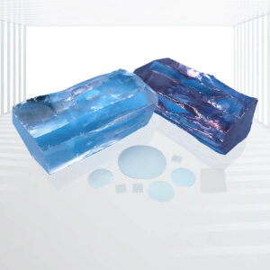
Germanium (Ge) Crystals
Exceptional Optical Properties:
Germanium crystals exhibit high transmittance and a high refractive index, making them suitable for optical components in Peer-to-Point communication systems.
The uniform transmittance ensures consistent performance and signal integrity.
Superior Semiconductor Characteristics:
Germanium is a semiconductor material with excellent electrical properties, allowing for efficient signal transmission and processing.
Its high radiation resistance ensures stable performance even in harsh environments.
Mechanical Strength and Durability:
Germanium substrates are mechanically strong, providing robustness and longevity in Peer-to-Point communication devices.
The ability to thin the substrates enables the creation of lighter and more compact devices.
Cost-Effective Solution:
Compared to other semiconductor materials like Gallium Arsenide (GaAs), Germanium is less expensive, offering cost savings in manufacturing Peer-to-Point communication systems.
Versatile Application Range:
Germanium crystals and substrates can be used in various components of Peer-to-Point communication systems, including infrared optics, solar cell substrates, and semiconductor devices.
Applications: Semiconductors, Infrared optics, Solar cell field, etc.
Our advanced manufacturing techniques ensure extremely low impurity levels in the crystalline Germanium, enhancing its performance in semiconductor devices. Each wafer is precisely “off-cut” towards the appropriate direction and packaged in a 1000-grade clean room using 100-grade bags to maintain cleanliness and quality.We provide Germanium crystals and substrates tailored to meet specific customer requirements, ensuring optimal performance in Peer-to-Point communication systems.
Specifications:
| Parameter Name | Value |
| Crystal Growth | CZ |
| Crystal Structure | Monocrystalline/Polycrystalline |
| Purity | ≥6N |
| Conductivity Type | n |
| Resistivity | 5-40 Ω·cm
1-5 Ω·cm >50 Ω·cm |
| Surface Finish | Ramax 0.2 μm to 4.0 μm (D7 to D46) |
| Transmission Spectrum | 2-14 μm |
| Coefficient of Refractive Index (dn/dT) | 400 x 10-6 K |
| Refractive Index 10.6 μm | 4.00462 |
| Refractive Index Homogeneity | ≤1.0 + 10-4 |
| Absorption Coefficient, 10.6 μm, (/cm) | ≤ 0.035 cm |
| Optical Transmittance, 10.6 μm | >46% |
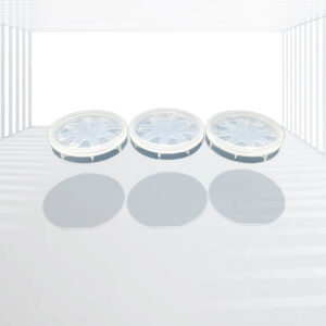
| Circular Disks | Monocrystalline: 3 ‒ 310mm
Polycrystal: 3 – 400mm Thickness: >0.5mm |
| Rectangular Sheets | Length x Width: 4×4~350×350mm
Thickness: >0.5mm Parallelism: <0.03mm |
| Lenses (Spherical/ Aspherical) | Diameter: 5-270mm ETV<0.03mm |
| Other Shapes | Available on request |
Features:
1.Exceptional Optical Properties:
- Germanium crystals exhibit high transmittance and a high refractive index, making them suitable for optical components in Peer-to-Point communication systems.
- The uniform transmittance ensures consistent performance and signal integrity.
2.Superior Semiconductor Characteristics:
- Germanium is a semiconductor material with excellent electrical properties, allowing for efficient signal transmission and processing.
- Its high radiation resistance ensures stable performance even in harsh environments.
3.Mechanical Strength and Durability:
- Germanium substrates are mechanically strong, providing robustness and longevity in Peer-to-Point communication devices.
- The ability to thin the substrates enables the creation of lighter and more compact devices.
4.Cost-Effective Solution:
- Compared to other semiconductor materials like Gallium Arsenide (GaAs), Germanium is less expensive, offering cost savings in manufacturing Peer-to-Point communication systems.
5.Versatile Application Range:
- Germanium crystals and substrates can be used in various components of Peer-to-Point communication systems, including infrared optics, solar cell substrates, and semiconductor devices.
Applications:
1.Semiconductors:
- Basic semiconductor materials: In the sixties and seventies of the 20th century, germanium was a typical semiconductor material and enjoyed the status of a national strategic material. Although with the advancement of technology, the basic application of silicon in the semiconductor field has gradually replaced the scarce and expensive germanium, the electron mobility and hole mobility of germanium are larger than that of silicon, making it suitable for ultra-high-speed transfer switching circuits.
- High-frequency, fast-low-noise field: In high-frequency, fast-low-noise applications, germanium devices perform far better than silicon devices.
- Modern semiconductor devices: Germanium is still used in the manufacture of a variety of semiconductor devices, such as thermistors, photoresistors, and semiconductor thermometers, for temperature measurement and automatic control of equipment.
2. Infrared optics
- Infrared optical materials: Germanium, as an infrared optical material, has the advantages of high infrared refractive index, wide range of infrared transmission band, small absorption coefficient, low dispersion and easy processing, especially suitable for the materials of windows, lenses, prisms and filters of thermal imagers and infrared radars and other infrared optical devices in military and major civilian use.
- Infrared detectors: Si-Ge alloys and single crystals of germanium doped with mercury, cadmium, copper and gallium are used in infrared detectors to improve the performance of infrared detection technology.
3. Solar cell field
- High-efficiency solar cell substrate: The manufacturing technology of high-efficiency multi-section solar cells with germanium as the substrate has been mature in foreign countries, and the photoelectric conversion efficiency in the laboratory has reached more than 40%, which is 2-3 times that of silicon solar cells. This kind of high-efficiency solar cells are widely used in solar power supply for space vehicles such as artificial satellites and space shuttles, and in terrestrial concentrated solar power generation systems.
陶瓷基板1-300x300.jpg)
陶瓷基板2-300x300.jpg "Kingwim Optics Thick Flim Metalized Beryllium Oxide Ceramic Substrates")
晶体和晶圆1-300x300.jpg)
晶体和晶圆2-300x300.jpg "Kingwim Optics SAW Quartz (SiO2) Crystals and Wafers")
 Crystals and Substrates")