 Crystals and Substrates")
 Crystals and Substrates")
1.jpg "Kingwim Optics Indium arsenide (InAs) Crystals and Substrates")
2.jpg "Kingwim Optics Indium arsenide (InAs) Crystals and Substrates")
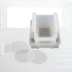
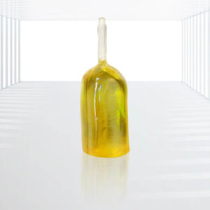
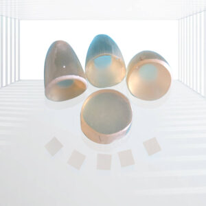
Indium arsenide (InAs) Crystals and Substrates
High Electron Mobility: InAs has a high electron mobility, enabling it to excel in high-frequency and high-speed electronic devices. This characteristic contributes to faster signal processing and transmission.
Direct Bandgap: Its direct bandgap structure allows for efficient optical transitions, making InAs ideal for optoelectronic devices such as photodetectors and lasers.
Tunable Properties: The bandgap of InAs can be tuned by alloying with other semiconductor materials, providing flexibility in device design and performance optimization.
Good Thermal Stability: Compared to some other semiconductor materials, InAs demonstrates good thermal stability, allowing it to operate in relatively high-temperature environments.
Low Noise Characteristics: InAs exhibits low noise properties, making it suitable for applications requiring high signal-to-noise ratios, such as low-noise amplifiers.
Applications: Optoelectronics, High-Speed Electronics, Solar Cells, Thermophotovoltaics, etc.
Indium Arsenide (InAs) is a III-V compound semiconductor material consisting of indium and arsenic. It exhibits a direct bandgap structure with a narrow bandgap energy, typically around 0.36 eV to 0.7 eV, depending on the measurement conditions. InAs crystals and substrates possess unique physical and electronic properties that make them attractive for various high-tech applications.
Specifications:
| Main performance parameters | |||||||
| Single crystal | adulterate | Conductive type | Carrier concentration
cm-3 |
Mobility (cm.)2/V.s) | Dislocation density (cm-2) | Standard substrates | |
| InAs | Intrinsics | N | 5*1016 | 2*104 | <5*104 | Φ2″×0.5mm
Φ3″×0.5mm |
|
| InAs | Sn | N | (5-20)*1017 | >2000 | <5*104 | Φ2″×0.5mm
Φ3″×0.5mm |
|
| InAs | Zn | P | (1-20) *1017 | 100-300 | <5*104 | Φ2″×0.5mm
Φ3″×0.5mm |
|
| InAs | S | N | (1-10)*1017 | >2000 | <5*104 | Φ2″×0.5mm
Φ3″×0.5mm |
|
| Dimensions (mm) | Dia50.8×0.5mm, 10×10×0.5mm, 10×5×0.5mm can be customized according to customer needs | ||||||
| Surface roughness | Surface roughness (Ra): <=5A can provide atomic particle microscopy (AFM) inspection report |
||||||
| polished | Single-sided or double-sided | ||||||
| wrap | Class 100 clean bag, Class 1000 clean room | ||||||
| structure | Cube a=6.058 A | ||||||
| Crystal orientation | <100> | ||||||
| melting point oC | 942 | ||||||
| Density g/cm3 | 5.66 | ||||||
| Bandgap width | 0.45 | ||||||
Advantages:
- High Electron Mobility: InAs has a high electron mobility, enabling it to excel in high-frequency and high-speed electronic devices. This characteristic contributes to faster signal processing and transmission.
- Direct Bandgap: Its direct bandgap structure allows for efficient optical transitions, making InAs ideal for optoelectronic devices such as photodetectors and lasers.
- Tunable Properties: The bandgap of InAs can be tuned by alloying with other semiconductor materials, providing flexibility in device design and performance optimization.
- Good Thermal Stability: Compared to some other semiconductor materials, InAs demonstrates good thermal stability, allowing it to operate in relatively high-temperature environments.
- Low Noise Characteristics: InAs exhibits low noise properties, making it suitable for applications requiring high signal-to-noise ratios, such as low-noise amplifiers.
Applications:
1.Optoelectronics:
- Photodetectors: InAs’s high absorption coefficient and direct bandgap make it ideal for infrared photodetectors, critical components in optical communication systems and night vision devices.
- Lasers: InAs-based lasers are used in optical fiber communications, medical equipment, and scientific instruments due to their high efficiency and tunable wavelength capabilities.
2.High-Speed Electronics:
- HEMTs (High Electron Mobility Transistors): The high electron mobility of InAs enables the fabrication of high-speed transistors for microwave and millimeter-wave applications.
- Integrated Circuits: InAs is being explored for use in advanced integrated circuits, particularly those requiring high-speed processing capabilities.
3.Solar Cells:
- InAs-based solar cells can harness infrared radiation, extending the spectral range of traditional silicon-based solar cells and potentially improving energy conversion efficiency.
4.Thermophotovoltaics:
- InAs-based thermophotovoltaic cells can convert thermal radiation into electricity, offering potential applications in waste heat recovery and space power systems.
Indium Arsenide (InAs) crystals and substrates offer a combination of exceptional physical and electronic properties that make them valuable materials for a wide range of high-tech applications, including optoelectronics, high-speed electronics, solar cells, quantum computing, and thermophotovoltaics.

3-300x300.jpg "Kingwim Optics SrLaAlO4 (Strontium Lanthanum Aluminate) Crystal Wafers")

1-300x300.jpg)
2-300x300.jpg "Kingwim Optics MgAl2O4 Substrates")