Wafers and Substrates")
 Wafers and Substrates")
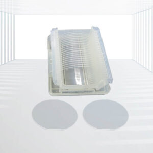
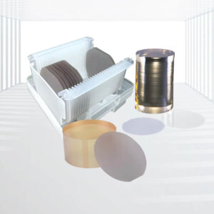
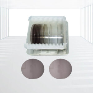
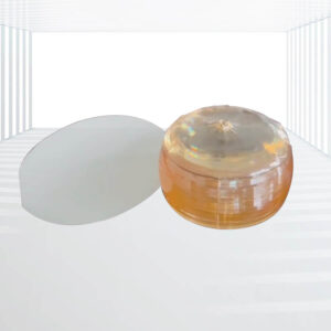
CZT (CdZnTe) Wafers and Substrates
High Purity: Achieved through rigorous purification processes, our CZT wafers boast a purity level exceeding 99.999999%, ensuring accurate and reliable detection.
Excellent Photoconductivity: Direct conversion of X-rays and gamma rays into electrical signals at room temperature, making them ideal for a wide range of detectors.
Wide Energy Range: Capable of detecting energies from 10KeV to 6MeV, covering the spectrum required for medical imaging, security screening, and industrial inspections.
Low Noise: Low dark current and high resistivity contribute to low noise levels, enhancing the signal-to-noise ratio and improving detection sensitivity.
Customizable: Available in various sizes and thicknesses to meet specific application requirements.
Applications: Medical Imaging, Astrophysics and High Energy Physics, Environmental Monitoring, Industrial Testing, Research & Education, etc.
Kingwin Optics’ CdZnTe (CZT) Wafers are precision-crafted from the highest purity CZT material, ensuring unparalleled performance in radiation detection and photon counting applications. Our wafers are grown using state-of-the-art crystal growth techniques, such as the Vertical Bridgman method, to minimize impurities and defects, resulting in superior dark current, resistance, and thermal stability.
Specifications:
| Materials | Cd1-xZnxTe,x=0.04 |
| Type | p-type |
| Size(mm3) | 14×14×1.3, 10×10×1 |
| Index of Crystal Face | (111), (211) |
| Orientation and Accuracy | Low index surface orientation, Orientation Accuracy ≤0.3° |
| Resistivity | ρ>106 Ω·cm |
| IR Transmission% | ≥60% |
| Infrared Imaging | Te inclusions≤ 2μm or Cd inclusions≤2μm |
| X-ray DCRC FWHM(FWHM) | ≤30 rad·s |
| Average Etch Pit density(EPD) | 1×10⁴/cm2 ~ 5×10⁴/cm2 |
| Surfaces Roughness | Ra≤0.5 nm |
Key Features:
- High Purity: Achieved through rigorous purification processes, our CZT wafers boast a purity level exceeding 99.999999%, ensuring accurate and reliable detection.
- Excellent Photoconductivity: Direct conversion of X-rays and gamma rays into electrical signals at room temperature, making them ideal for a wide range of detectors.
- Wide Energy Range: Capable of detecting energies from 10KeV to 6MeV, covering the spectrum required for medical imaging, security screening, and industrial inspections.
- Low Noise: Low dark current and high resistivity contribute to low noise levels, enhancing the signal-to-noise ratio and improving detection sensitivity.
- Customizable: Available in various sizes and thicknesses to meet specific application requirements.
Applications:
1.Medical Imaging:
- As the core material of X-ray photon detectors, it is used in medical devices such as CT (computed tomography) and SPECT (single photon emission computed tomography) to provide high-definition medical images.
2.Astrophysics and High Energy Physics:
- It is used to detect high-energy particles and rays in the universe, such as gamma rays, X-rays, etc.
- In high-energy physics experiments, it is used to build sophisticated detector systems.
3.Environmental Monitoring:
- Detect radioactive contamination and heavy metal contamination in the environment such as soil and water quality.
- In environmental protection departments or research institutes, it is used to monitor environmental radiation levels.
4.Industrial Testing:
- In the field of non-destructive testing, it is used to detect defects and structures inside materials, such as cracks and inclusions in metals, ceramics and other materials.
- It is used for security inspections, such as cargo screening at airports, ports, etc.
5.Research & Education:
- In scientific research and educational institutions in the fields of physics, materials science, electronic engineering, etc., for experiments and research.
All Kingwin Optics CZT wafers undergo rigorous quality control measures, including X-ray diffraction, electrical testing, and surface analysis, to ensure compliance with international standards and customer specifications.


")