Showing 33–46 of 46 results

  • Kingwim Optics SAW Grade LiTaO3 WafersKingwim Optics SAW Grade LiTaO3 Wafers

    SAW Grade LiTaO3 Wafers

    Exceptional Piezoelectric Properties: Efficient energy transformation in SAW devices.

    Good Mechanical and Electrical Coupling:Ensures reliable performance in various applications.

    Stable Temperature Coefficient: Maintains performance consistency across temperature variations.

    Applications: Q-switch in Laser Applications, Pyroelectric Detectors in Infrared Applications, Filters and Resonators in Electronics, etc.

  • Kingwim Optics SAW Quartz (SiO2) Crystals and WafersKingwim Optics SAW Quartz (SiO2) Crystals and Wafers

    SAW Quartz (SiO2) Crystals and Wafers

    High Thermal Stability: Maintains stable piezoelectric properties at room temperature.

    High Mechanical Strength: Durable and resistant to mechanical stress.

    High Quality Factor: Ensures precise and efficient signal processing.

    High Rigidity and Good Dynamic Characteristics: Provides robustness and reliability in dynamic applications.

    No Pyroelectric and Ferroelectric Effect: Offers stable performance without thermal-induced changes.

    Excellent Insulation Properties: Ensures minimal electrical interference and high performance.

    Applications: Resonators, High-Frequency Oscillators, Filters, Navigation and Remote Control, Telemetry, Electronics and Electric Equipment, etc.

  • Kingwim Optics SGGG (Substituted GGG) Single Crystals and WafersKingwim Optics SGGG (Substituted GGG) Single Crystals and Wafers

    SGGG (Substituted GGG) Single Crystals and Wafers

    Larger Lattice Constant: SGGG offers a larger lattice constant compared to GGG, which can be beneficial for applications requiring better lattice matching with epitaxial films or higher magneto-optical performance.

    Improved Optical Properties: With low optical loss (<0.1%/cm), SGGG wafers provide superior optical transparency, making them ideal for applications where optical quality is paramount.

    High Thermal Conductivity: The high thermal conductivity of SGGG (7.4 W m-1 K-1) ensures efficient heat dissipation during high-power operation, reducing thermal stress and improving device reliability.

    High Laser Damage Threshold: With a laser damage threshold exceeding 1 GW/cm², SGGG crystals and wafers can withstand intense laser irradiation, making them suitable for high-power laser systems.

    Customizable Compositions: The substitution of ions allows for tailored compositions to optimize specific properties, such as lattice constants, thermal expansion coefficients, or magneto-optical effects.

    Surface Quality: Kingwin Optics ensures that SGGG wafers are polished to a high degree of smoothness, typically with a surface roughness of Ra ≤ 5Å, to support defect-free epitaxial growth.

    Applications: High-Power Laser Systems, Magnetic Bubble Memory, Integrated Optics, Specialized Research & Development, etc.

  • Kingwim Optics Silicon (Si) Crystals and WafersKingwim Optics Silicon (Si) Crystals and Wafers

    Silicon (Si) Crystals and Wafers

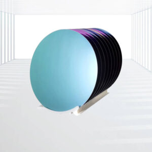
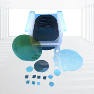
    High-Purity Polycrystalline Silicon Ingots:Silicon wafers are made from high-purity polycrystalline silicon ingots, ensuring minimal impurities and consistent material properties.

    Controlled Manufacturing Process:The manufacturing process follows a controlled and organized sequence, including crystal growth, slicing, chamfering/grinding (lapping), surface etching/polishing, cleaning, inspection, packaging, and other processes, ensuring high-quality wafers.

    Customizable Doping:Doping with designed concentrations can be introduced into the silicon crystal lattice to alter its electrical properties and create regions with specific conductivity (n-type or p-type) required for semiconductor devices.

    Versatile Platform for Thin Film Deposition:Si wafers serve as excellent platforms for the deposition of various thin films to achieve specific functions, making them versatile for a wide range of applications.

    Multiple Applications:Kingwin Optics’ Silicon (Si) wafers and substrates are used as substrates for GaN (Gallium Nitride) epitaxial film growth, semiconductors, and solar cells, demonstrating their versatility and wide range of applications.

    Applications: GaN Epitaxial Film Growth, Semiconductors, Solar Cells, etc.

  • Kingwim Optics Silicon Carbide (SiC) CeramicsKingwim Optics Silicon Carbide (SiC) Ceramics

    Silicon Carbide (SiC) Ceramics

    High Hardness and Wear Resistance: SiC ceramics have a hardness of 9.2 on the Mohs scale, making them highly resistant to abrasion and wear.

    High Thermal Conductivity: SiC has excellent thermal conductivity, allowing efficient heat dissipation in high-temperature environments.

    Low Thermal Expansion: SiC exhibits low thermal expansion, ensuring dimensional stability under temperature fluctuations.

    High Temperature Strength: SiC ceramics maintain their strength at elevated temperatures, making them suitable for high-temperature applications.

    Chemical Inertness: Resistant to chemical attack by acids, alkalis, and molten salts, SiC ceramics are ideal for corrosive environments.

    Electrical Properties: Depending on the doping and manufacturing process, SiC can exhibit semiconductor properties.

    Applications: Aerospace and Defense, Electronics, Mechanical Seals and Bearings, Heat Exchangers, Kiln Furniture, Chemical Processing, etc.

  • Kingwim Optics Silicon Carbide (SiC) Crystals and WafersKingwim Optics Silicon Carbide (SiC) Crystals and Wafers

    Silicon Carbide (SiC) Crystals and Wafers

    Exceptional Thermal Conduction: SiC has exceptional thermal conductivity, allowing for efficient heat dissipation in high-power devices. This results in reduced cooling necessities and improved device reliability.

    Superior Mechanical Resilience: With high hardness and lightweight nature, SiC wafers are robust and durable, making them ideal for harsh operating conditions.

    Broad Bandgap: The broad bandgap of SiC enables the production of devices with higher breakdown voltages and lower leakage currents, essential for high-voltage applications.

    Large Electric Field Breakdown Strength: SiC’s ability to withstand large electric fields allows for the development of compact, high-efficiency power devices.

    High-Temperature Endurance: SiC’s endurance to withstand high temperatures makes it suitable for applications where traditional silicon devices would fail.

    Improved Switching Speeds: SiC-based power devices boast swifter switching speeds, leading to increased efficiency and reduced power loss.

    Applications: High-Frequency Power Electronic Devices, RF Transistors, Optoelectronic Devices, Extreme Environmental Applications, etc.

  • Kingwim Optics SrLaAlO4 (Strontium Lanthanum Aluminate) Crystal WafersKingwim Optics SrLaAlO4 (Strontium Lanthanum Aluminate) Crystal Wafers

    SrLaAlO4 (Strontium Lanthanum Aluminate) Crystal Wafers

    Perovskite Structure: Shares similarities with SrTiO3 but offers a more stable structure with fewer defects.

    Lattice Match: Excellent compatibility with high-temperature superconductors like Yttrium Barium Copper Oxide (YBCO), facilitating the growth of high-Tc superconducting films.

    Thermal Expansion: Lower thermal expansion coefficients compared to other perovskite crystals, which improves lattice matching and reduces stress during film growth.

    Dielectric Properties: Low dielectric constants make it superior for microwave and high-frequency applications.

    Applications: High-Temperature Superconductors, Microwave and High-Frequency Devices, Epitaxial Growth, Advanced Material Research, etc.

  • Kingwim Optics SrTiO3 SubstratesKingwim Optics SrTiO3 Substrates

    SrTiO3 Substrates

    Lattice Match:

    Lattice constant: 3.905Å, closely matching high Tc superconductive material YBCO (3.88 Å).

    Facilitates the epitaxial growth of HTS and many oxide thin films.

    Crystal Structure:

    Twin-less crystal structure.

    Excellent physical and mechanical properties for film growth.

    High Tc Films Compatibility:

    Suitable for various high Tc films such as YBCO, Bi-system, and La-system.

    Wide Applications:

    Used for special optical windows and high-quality sputtering targets.

    Compatible with multiple film growth technologies.

    Applications: High-Temperature Superconductors (HTS), Optical Windows, Sputtering Targets, etc.

  • Kingwim Optics TGG (Terbium Gallium Garnet) Crystals and SubstratesKingwim Optics TGG (Terbium Gallium Garnet) Crystals and Substrates

    TGG (Terbium Gallium Garnet) Crystals and Substrates

    High Faraday Rotation: TGG exhibits an exceptionally high Faraday rotation, making it an ideal material for optical isolators, circulators, and other magneto-optical devices. This high rotation enables efficient polarization control and isolation of optical signals.

    Low Optical Absorption: With low optical absorption across a wide spectral range, TGG substrates provide excellent optical transparency, ensuring minimal loss of light during transmission. This feature is crucial for maintaining signal integrity in optical communication systems and other optical applications.

    Good Thermal Stability: TGG demonstrates good thermal stability, allowing it to withstand temperature fluctuations without significant degradation of its optical or magneto-optical properties. This characteristic ensures reliable performance even under demanding operating conditions.

    High Laser Damage Threshold: TGG crystals possess a high laser damage threshold, enabling them to withstand intense laser irradiation without damage. This feature makes them suitable for use in high-power laser systems and other applications where exposure to high-intensity laser light is expected.

    High Chemical Stability: TGG exhibits high chemical stability, resisting corrosion and other forms of degradation when exposed to various environments. This property ensures long-term durability and reliability in a wide range of applications.

    Applications: Optical Isolators and Circulators, High-Power Laser Systems, Magneto-Optical Recording, Integrated Optics, Research and Development, etc.

  • Kingwim Optics Thick Flim Metalized Beryllium Oxide Ceramic SubstratesKingwim Optics Thick Flim Metalized Beryllium Oxide Ceramic Substrates

    Thick Flim Metalized Beryllium Oxide Ceramic Substrates

    High Ruggedness: Robust construction minimizes the possibility of outgassing.

    Nickel Plating: Ensures durability without blistering.

    Versatility: Suitable for various applications requiring high thermal and electrical performance.

    Applications: Wire Bonding Platforms, Microwave PCBs, Thermoelectric Coolers (TEC) for Lasers, Hybrid Integrated Circuits (HIC) for Automotive, High-Power Semiconductor Modules, Hermetic Electrical Packaging, etc.

  • Kingwim Optics TiO2 (Titanium dioxide) Crystals and SubstratesKingwim Optics TiO2 (Titanium dioxide) Crystals and Substrates

    TiO2 (Titanium dioxide) Crystals and Substrates

    Excellent Supportive Platform: TiO2 substrates offer an ideal platform for growing thin films of various materials, particularly VO2, which can be difficult to grow on other substrates.

    Large Birefringence and Refractive Index: Optical grade rutile TiO2 single crystal substrates exhibit large birefringence and a high refractive index, making them suitable for spectral prism and polarizing devices such as optical isolators and beam splitters.

    Superior Physical and Chemical Stabilities: Compared to YVO4, TiO2 crystals demonstrate better physical and chemical stabilities, ensuring reliable performance in various applications.

    Applications: Thin Film Growth, Spectral Prism and Polarizing Devices, Optical Components, etc.

  • Kingwim Optics YAlO3 (YAP) Crystals and SubstratesKingwim Optics YAlO3 (YAP) Crystals and Substrates

    YAlO3 (YAP) Crystals and Substrates

    Optical Properties:

    Transparency: Wide band gap making it suitable for near-infrared (NIR) applications.

    Dopants: Rare earth and transition-metal ions can be doped for specialized applications such as lasers.

    Material Properties:

    High-Temperature Superconductors (HTS): Suitable for the growth of HTS thin films.

    II-V Nitride and Oxide Films: Provides a reliable substrate for these materials.

    Applications: High-Temperature Superconducting (HTS) Thin Films, II-V Nitride and Oxide Films, Near-Infrared (NIR) Applications, Lasers, etc.

  • Kingwim Optics YSZ (Yttria Stabilized Zirconia) Crystals and SubstratesKingwim Optics YSZ (Yttria Stabilized Zirconia) Crystals and Substrates

    YSZ (Yttria Stabilized Zirconia) Crystals and Substrates

    Moderate Cost: YSZ substrates offer a cost-effective solution for various applications.

    Wear-Resistance: The material exhibits high wear resistance, making it suitable for demanding applications.

    Good Match with Oxides: YSZ substrates have good compatibility with multiple single and multiplication oxides, allowing for versatile use in different applications.

    Early Application in Superconducting Thin Films: YSZ was one of the earliest materials used for stabilizing high-temperature superconducting thin films of YBCO.

    Applications: Solid Oxide Fuel Cells (SOFCs), Thermal Barrier Coatings (TBCs), Oxygen Sensors, Medical Implants, Electronics, etc.

  • Kingwim Optics Zinc oxide (ZnO) Crystal and SubstratesKingwim Optics Zinc oxide (ZnO) Crystal and Substrates

    Zinc oxide (ZnO) Crystal and Substrates

    Wide Bandgap: With a bandgap of 3.4 eV, ZnO is suitable for manifold blue and violet optoelectronic applications as well as UV devices.

    Competitive Edge: The availability of large-size ZnO crystals offers a competitive advantage over other materials like GaN.

    Optimal GaN Film Growth: ZnO substrates have a wurtzite structure with lattice constants well-matched to GaN, resulting in minimal lattice mismatch and optimal film growth.

    Lattice Stress Absorption: ZnO is a soft compliant material that effectively absorbs lattice stress, protecting the growing GaN thin film.

    Customized Solutions: Kingwin Optics offers customized high-quality ZnO crystal substrates and wafers to meet specific application requirements.

    Applications: Optoelectronic Devices, UV Devices, Thin Film Growth, Research and Development, etc.