-
薄膜1-300x300.jpg)
薄膜2-300x300.jpg)
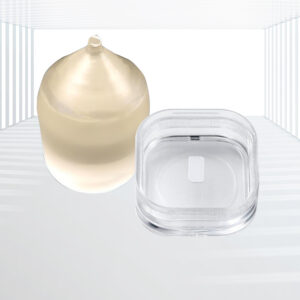
Wide Direct Bandgap: GaN has a wide direct bandgap of 3.4 eV, which enables efficient emission and absorption of light at short wavelengths, making it ideal for optoelectronic applications.
Stable Physical and Chemical Properties: The strong atomic bonds of GaN contribute to its stable physical and chemical properties, ensuring reliability and durability in various applications.
Exceptional Thermal Properties: GaN exhibits exceptional thermal properties, allowing it to perform well in high-temperature environments, making it suitable for high-temperature semiconductor devices.
Excellent Radiation Resistance: GaN crystals and wafers have excellent radiation resistance, making them suitable for applications in environments with high levels of radiation.
Customizable Options: Kingwin Optics offers custom GaN wafers and substrates, with options including N-type and semi-insulating types, providing tailored solutions for various applications.
Applications: LED Applications, Laser Diodes, High-Power and High-Frequency Electronic Devices, High-Temperature Semiconductor Devices, etc.
-
晶体和晶圆1-300x300.jpg)
晶体和晶圆2-300x300.jpg)
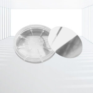
High Electromechanical Coupling Factor: LGS crystal has an electromechanical coupling factor of 15.8%, higher than that of quartz crystal. This indicates its high efficiency in converting electrical energy into mechanical energy.
Lower Propagation Velocities: The surface acoustic wave propagation velocity in LGS crystal is much lower compared to other materials. This allows for smaller geometrical dimensions of filters operating at the same center frequency, which aligns with the trend towards denser integration of modern electronics and reduces production costs.
High Thermal Stability: Devices made from langasite crystal can operate at high temperatures up to 900°C, making them suitable for high-temperature applications.
Applications: Surface Acoustic Wave (SAW) Devices, Bulk Acoustic Wave (BAW) Devices, High-Temperature Applications, etc.
-
晶体和晶圆1-300x300.jpg)
晶体和晶圆2-300x300.jpg)
High Thermal Stability: Maintains stable piezoelectric properties at room temperature.
High Mechanical Strength: Durable and resistant to mechanical stress.
High Quality Factor: Ensures precise and efficient signal processing.
High Rigidity and Good Dynamic Characteristics: Provides robustness and reliability in dynamic applications.
No Pyroelectric and Ferroelectric Effect: Offers stable performance without thermal-induced changes.
Excellent Insulation Properties: Ensures minimal electrical interference and high performance.
Applications: Resonators, High-Frequency Oscillators, Filters, Navigation and Remote Control, Telemetry, Electronics and Electric Equipment, etc.
-


Larger Lattice Constant: SGGG offers a larger lattice constant compared to GGG, which can be beneficial for applications requiring better lattice matching with epitaxial films or higher magneto-optical performance.
Improved Optical Properties: With low optical loss (<0.1%/cm), SGGG wafers provide superior optical transparency, making them ideal for applications where optical quality is paramount.
High Thermal Conductivity: The high thermal conductivity of SGGG (7.4 W m-1 K-1) ensures efficient heat dissipation during high-power operation, reducing thermal stress and improving device reliability.
High Laser Damage Threshold: With a laser damage threshold exceeding 1 GW/cm², SGGG crystals and wafers can withstand intense laser irradiation, making them suitable for high-power laser systems.
Customizable Compositions: The substitution of ions allows for tailored compositions to optimize specific properties, such as lattice constants, thermal expansion coefficients, or magneto-optical effects.
Surface Quality: Kingwin Optics ensures that SGGG wafers are polished to a high degree of smoothness, typically with a surface roughness of Ra ≤ 5Å, to support defect-free epitaxial growth.
Applications: High-Power Laser Systems, Magnetic Bubble Memory, Integrated Optics, Specialized Research & Development, etc.
-


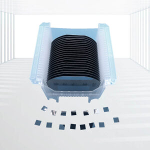
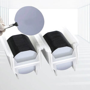
High-Purity Polycrystalline Silicon Ingots:Silicon wafers are made from high-purity polycrystalline silicon ingots, ensuring minimal impurities and consistent material properties.
Controlled Manufacturing Process:The manufacturing process follows a controlled and organized sequence, including crystal growth, slicing, chamfering/grinding (lapping), surface etching/polishing, cleaning, inspection, packaging, and other processes, ensuring high-quality wafers.
Customizable Doping:Doping with designed concentrations can be introduced into the silicon crystal lattice to alter its electrical properties and create regions with specific conductivity (n-type or p-type) required for semiconductor devices.
Versatile Platform for Thin Film Deposition:Si wafers serve as excellent platforms for the deposition of various thin films to achieve specific functions, making them versatile for a wide range of applications.
Multiple Applications:Kingwin Optics’ Silicon (Si) wafers and substrates are used as substrates for GaN (Gallium Nitride) epitaxial film growth, semiconductors, and solar cells, demonstrating their versatility and wide range of applications.
Applications: GaN Epitaxial Film Growth, Semiconductors, Solar Cells, etc.
-


Exceptional Thermal Conduction: SiC has exceptional thermal conductivity, allowing for efficient heat dissipation in high-power devices. This results in reduced cooling necessities and improved device reliability.
Superior Mechanical Resilience: With high hardness and lightweight nature, SiC wafers are robust and durable, making them ideal for harsh operating conditions.
Broad Bandgap: The broad bandgap of SiC enables the production of devices with higher breakdown voltages and lower leakage currents, essential for high-voltage applications.
Large Electric Field Breakdown Strength: SiC’s ability to withstand large electric fields allows for the development of compact, high-efficiency power devices.
High-Temperature Endurance: SiC’s endurance to withstand high temperatures makes it suitable for applications where traditional silicon devices would fail.
Improved Switching Speeds: SiC-based power devices boast swifter switching speeds, leading to increased efficiency and reduced power loss.
Applications: High-Frequency Power Electronic Devices, RF Transistors, Optoelectronic Devices, Extreme Environmental Applications, etc.

薄膜1-300x300.jpg)
薄膜2-300x300.jpg)
晶体和晶圆1-300x300.jpg)
晶体和晶圆2-300x300.jpg)
晶体和晶圆1-300x300.jpg)
晶体和晶圆2-300x300.jpg)
