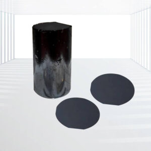
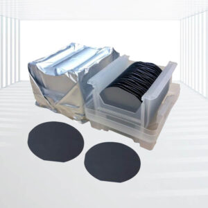
CZT (CdZnTe) Wafers and Substrates
High Purity: Achieved through rigorous purification processes, our CZT wafers boast a purity level exceeding 99.999999%, ensuring accurate and reliable detection.
Excellent Photoconductivity: Direct conversion of X-rays and gamma rays into electrical signals at room temperature, making them ideal for a wide range of detectors.
Wide Energy Range: Capable of detecting energies from 10KeV to 6MeV, covering the spectrum required for medical imaging, security screening, and industrial inspections.
Low Noise: Low dark current and high resistivity contribute to low noise levels, enhancing the signal-to-noise ratio and improving detection sensitivity.
Customizable: Available in various sizes and thicknesses to meet specific application requirements.
Applications: Medical Imaging, Astrophysics and High Energy Physics, Environmental Monitoring, Industrial Testing, Research & Education, etc.


