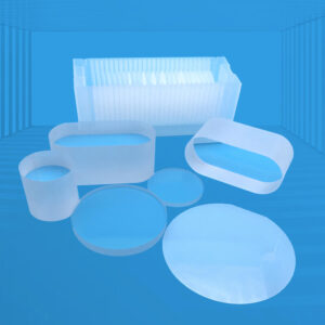
Sapphire (Al2O3) Substrates and Wafers
Versatility: Sapphire Wafers and Substrates are suitable for a wide range of applications, including III-V and II-VI compound thin film growth for semiconductors, Light Emitting Diodes (LEDs), high-temperature superconducting (HTSC) thin films, Microelectronic ICs (Silicon on Sapphire Integrated Circuit, SOS), Hybrid Microelectronic applications, and ferromagnetic/ferroelectric thin film growth.
Uniform Dielectric Constants: A-plane Sapphire Substrates and Wafers offer uniform dielectric constants and high electrical insulation, making them suitable alternatives for Hybrid Microelectronic applications, including HIC and MCM.
High-Speed Silicon On Sapphire (SOS): R-plane Sapphire Substrates and Wafers are ideal for the hetero-epitaxial deposition of silicon for Microelectronic ICs, enabling high-speed performance.
MOCVD Growth: C-plane Sapphire Substrates and Wafers are mainstream options for Metal Organic Chemical Vapor Deposition (MOCVD) growth of a series of III-V and II-VI compound thin films, including GaN, AlN, AlGaN, and InGaN, used in manufacturing blue, violet, and white light-emitting diodes (LEDs) and blue laser diodes (LDs).
Ferroelectric Thin Film Growth: C-plane Sapphire Substrates and Wafers are also suitable for the growth of ferroelectric thin films, such as (Pb, La)(Zr, Ti)O3 (PLZT), making them candidates for manufacturing new functional electronics.
Ferromagnetic Thin Film Growth: M-Plane Sapphire Substrates and Wafers are competent in the ferromagnetic thin film growth of Mn1−xS and other materials, making them suitable for applications such as solar-blind ultraviolet detection.
Applications: Semiconductors, Light Emitting Diodes (LEDs), High-Temperature Superconductors, Microelectronic ICs, Hybrid Microelectronic Applications, Functional Electronics, etc.

3-300x300.jpg)
