 Crystals and Wafers")
Silicon (Si) Crystals and Wafers
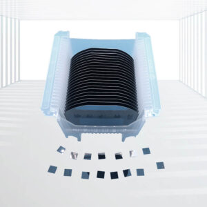
High-Purity Polycrystalline Silicon Ingots:Silicon wafers are made from high-purity polycrystalline silicon ingots, ensuring minimal impurities and consistent material properties.
Controlled Manufacturing Process:The manufacturing process follows a controlled and organized sequence, including crystal growth, slicing, chamfering/grinding (lapping), surface etching/polishing, cleaning, inspection, packaging, and other processes, ensuring high-quality wafers.
Customizable Doping:Doping with designed concentrations can be introduced into the silicon crystal lattice to alter its electrical properties and create regions with specific conductivity (n-type or p-type) required for semiconductor devices.
Versatile Platform for Thin Film Deposition:Si wafers serve as excellent platforms for the deposition of various thin films to achieve specific functions, making them versatile for a wide range of applications.
Multiple Applications:Kingwin Optics’ Silicon (Si) wafers and substrates are used as substrates for GaN (Gallium Nitride) epitaxial film growth, semiconductors, and solar cells, demonstrating their versatility and wide range of applications.
Applications: GaN Epitaxial Film Growth, Semiconductors, Solar Cells, etc.