Showing all 2 results

  • Kingwim Optics GGG Substrates and WafersKingwim Optics GGG Substrates and Wafers

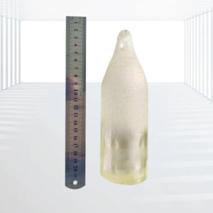
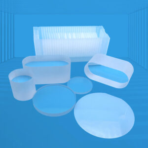
    GGG Substrates and Wafers

    Crystal Structure & Purity: Our GGG substrates and wafers feature a cubic crystal structure with a lattice constant of a=12.376Å, ensuring excellent structural match with YIG and BIG thin film magneto-optical materials. The purity level of 99.95% guarantees superior performance and reliability.

    Thermal Expansion Coefficient: The thermal expansion coefficient of GGG is carefully controlled to match that of the epitaxial films, minimizing stress during thermal cycling and ensuring stable device performance over a wide temperature range.

    Chemical Stability: GGG exhibits excellent chemical stability, resistant to decomposition and corrosion during the high-temperature epitaxial growth processes, preserving the quality of the deposited films.

    Optical Properties: With a refractive index of 1.95, GGG substrates and wafers are ideal for applications requiring precise optical control, such as optical isolators and waveguides.

    Surface Quality: The wafers are polished to a surface roughness of Ra≤5Å (5×5µm), ensuring smooth surfaces for defect-free epitaxial growth and enhanced device performance.

    Customization: Kingwin Optics offers customized GGG substrates and wafers in various dimensions, thicknesses, and orientations to meet the specific requirements of our customers.

    Application Areas: Magneto-Optical Devices, Microwave Devices, Magnetic Bubble Memory, Integrated Optics, etc.

  • Kingwim Optics Sapphire (Al2O3) Substrates and WafersKingwim Optics Sapphire (Al2O3) Substrates and Wafers

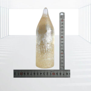
    Sapphire (Al2O3) Substrates and Wafers

    Versatility: Sapphire Wafers and Substrates are suitable for a wide range of applications, including III-V and II-VI compound thin film growth for semiconductors, Light Emitting Diodes (LEDs), high-temperature superconducting (HTSC) thin films, Microelectronic ICs (Silicon on Sapphire Integrated Circuit, SOS), Hybrid Microelectronic applications, and ferromagnetic/ferroelectric thin film growth.

    Uniform Dielectric Constants: A-plane Sapphire Substrates and Wafers offer uniform dielectric constants and high electrical insulation, making them suitable alternatives for Hybrid Microelectronic applications, including HIC and MCM.

    High-Speed Silicon On Sapphire (SOS): R-plane Sapphire Substrates and Wafers are ideal for the hetero-epitaxial deposition of silicon for Microelectronic ICs, enabling high-speed performance.

    MOCVD Growth: C-plane Sapphire Substrates and Wafers are mainstream options for Metal Organic Chemical Vapor Deposition (MOCVD) growth of a series of III-V and II-VI compound thin films, including GaN, AlN, AlGaN, and InGaN, used in manufacturing blue, violet, and white light-emitting diodes (LEDs) and blue laser diodes (LDs).

    Ferroelectric Thin Film Growth: C-plane Sapphire Substrates and Wafers are also suitable for the growth of ferroelectric thin films, such as (Pb, La)(Zr, Ti)O3 (PLZT), making them candidates for manufacturing new functional electronics.

    Ferromagnetic Thin Film Growth: M-Plane Sapphire Substrates and Wafers are competent in the ferromagnetic thin film growth of Mn1−xS and other materials, making them suitable for applications such as solar-blind ultraviolet detection.

    Applications: Semiconductors, Light Emitting Diodes (LEDs), High-Temperature Superconductors, Microelectronic ICs, Hybrid Microelectronic Applications, Functional Electronics, etc.