Gallium Antimonide (GaSb) Crystals and Substrates
Excellent physical and chemical properties:
GaSb belongs to group III-V compound semiconductors with a sphalerite structure and direct bandgap characteristics, with a bandgap width of 0.725 eV (300 K) and a lattice constant of 0.60959 nm.
GaSb single crystals have a high critical yield stress (15.8 N/mm²) and a low dislocation density (no more than 10³ order of magnitude), which makes them suitable for the fabrication of high-performance optoelectronic devices.
Good lattice matching:
The band gap of GaSb covers a variety of ternary and quaternary III.-V compound solid solutions in a wide spectral range (0.8~4.3μm), and the epitaxial growth of the above solid solution materials using GaSb as a substrate material can effectively reduce the stress and defects caused by lattice mismatch.
High photoelectric conversion efficiency:
Te-doped GaSb can be used to prepare thermophotovoltaic devices, tandem solar cells and microwave devices with high photoelectric conversion efficiency. These devices excel in photoelectric conversion efficiency and stability.
Various preparation methods:
The preparation of GaSb mainly includes the improved Straight Pull Method (CZ), Vertical Gradient Solidification Method (VGF) and Vertical Bridgeman Method (VB) such as Liquid Seal Straight Pull Method (LEC), Hydrogen Reduction Method, etc. Each of these methods has its own advantages and disadvantages, but all of them can meet the growth needs of GaSb crystals to varying degrees.
Customizability:
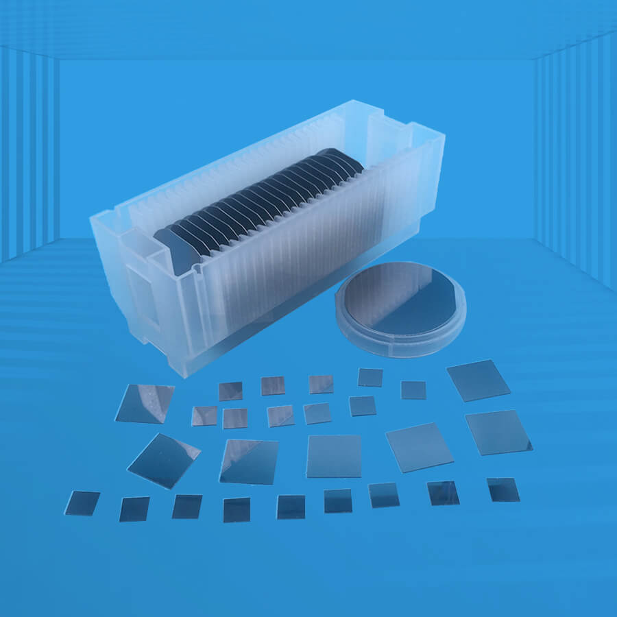
GaSb crystals and substrates can be customized according to customer needs, including different doping types (undoped, Zn-doped, Te-doped) and size specifications to meet the needs of different application scenarios.
Applications: Infrared Detectors & Lasers, Thermophotovoltaic devices, Solar Cells, Microwave Devices, etc.
Gallium Antimonide (GaSb), not GaAs as mentioned in the first sentence, is a substrate material used for the epitaxial growth of heterostructures, particularly suited for optoelectronic applications. Its lattice constant aligns well with various ternary, quaternary, and III-V compound solid solutions, which have a bandgap range of 0.8 to 4.3 micrometers. This compatibility makes GaSb an excellent choice for infrared optical fiber transmission. Additionally, GaSb is anticipated to have promising applications in the microwave field due to its higher lattice-restricted mobility compared to GaAs.
Specifications:
| Main performance parameters | |||||||
| Single crystal | adulterate | Conductive type | Carrier concentration
cm-3 |
Mobility (cm.)2/V.s) | Dislocation density (cm-2) | Standard substrates | |
| GaSb | Intrinsics | P | (1-2)*1017 | 600-700 | 《1*104 | Φ2″×0.5mm
Φ3″×0.5mm |
|
| GaSb | Zn | P | (5-100)*1017 | 200-500 | 《1*104
|
Φ2″×0.5mm
Φ3″×0.5mm |
|
| GaSb | Te | N | (1-20)´1017 | 2000-3500 | 《1*104 | Φ2″×0.5mm
Φ3″×0.5mm |
|
| Dimensions (mm) | Dia50.8×0.5mm, 10×10×0.5mm, 10×5×0.5mm can be customized according to customer needs | ||||||
| Surface roughness | Surface roughness (Ra): <=5A can provide atomic particle microscopy (AFM) inspection report |
||||||
| polished | Single-sided or double-sided | ||||||
| wrap | Class 100 clean bag, Class 1000 clean room | ||||||
| structure | Cube a=6.094A | ||||||
| Crystal orientation | <100> | ||||||
| melting point oC | 712 | ||||||
| Density g/cm3 | 5.53 | ||||||
| Bandgap width | 0.67 | ||||||
Features:
1.Excellent physical and chemical properties:
- GaSb belongs to group III-V compound semiconductors with a sphalerite structure and direct bandgap characteristics, with a bandgap width of 0.725 eV (300 K) and a lattice constant of 0.60959 nm.
- GaSb single crystals have a high critical yield stress (15.8 N/mm²) and a low dislocation density (no more than 10³ order of magnitude), which makes them suitable for the fabrication of high-performance optoelectronic devices.
2.Good lattice matching:
- The band gap of GaSb covers a variety of ternary and quaternary III.-V compound solid solutions in a wide spectral range (0.8~4.3μm), and the epitaxial growth of the above solid solution materials using GaSb as a substrate material can effectively reduce the stress and defects caused by lattice mismatch.
3.High photoelectric conversion efficiency:
- Te-doped GaSb can be used to prepare thermophotovoltaic devices, tandem solar cells and microwave devices with high photoelectric conversion efficiency. These devices excel in photoelectric conversion efficiency and stability.
4.Various preparation methods:
- The preparation of GaSb mainly includes the improved Straight Pull Method (CZ), Vertical Gradient Solidification Method (VGF) and Vertical Bridgeman Method (VB) such as Liquid Seal Straight Pull Method (LEC), Hydrogen Reduction Method, etc. Each of these methods has its own advantages and disadvantages, but all of them can meet the growth needs of GaSb crystals to varying degrees.
5.Customizability:
- GaSb crystals and substrates can be customized according to customer needs, including different doping types (undoped, Zn-doped, Te-doped) and size specifications to meet the needs of different application scenarios.
Applications:
1.Infrared Detectors & Lasers:
- GaSb is often used as a substrate material for infrared detectors and lasers of 8~14μm and larger than 14μm. These devices have a wide range of applications in military, industrial, medical, and other fields.
2.Thermophotovoltaic devices:
- Te-doped GaSb can be used to fabricate thermophotovoltaic devices that can use infrared light emitted by fossil fuels, isotopes, and nuclear energy for photovoltaic interaction, thereby freeing themselves from sunlight dependence.
3.Solar Cells:
- GaSb-based solar cells have high photoelectric conversion efficiency and stability, which is one of the ideal materials for manufacturing high-efficiency solar cells. In particular, the conversion efficiency of GaAs/GaSb tandem solar cells can exceed 30%.
4.Microwave Devices:
- GaSb can also be used to prepare microwave devices, which play an important role in communications, radar, and other fields.
Kingwin Optics provides customized GaSb crystals and substrates tailored to customers’ specifications, with a maximum diameter of 3 inches. They offer three types of GaSb materials: non-doping, Zinc (Zn) doped, and Tellurium (Te) doped. All substrates undergo rigorous testing and are packaged in a class 1000 clean room and class 100 bags to ensure their quality and cleanliness.

1.jpg)

2.jpg)


-300x300.jpg)

1-300x300.jpg)