薄膜1.jpg "Kingwim Optics GaN (Gallium Nitride) Crystals and Wafers")
薄膜2.jpg "Kingwim Optics GaN (Gallium Nitride) Crystals and Wafers")
薄膜3.jpg "Kingwim Optics GaN (Gallium Nitride) Crystals and Wafers")
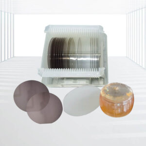
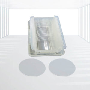
GaN (Gallium Nitride) Crystals and Wafers
Wide Direct Bandgap: GaN has a wide direct bandgap of 3.4 eV, which enables efficient emission and absorption of light at short wavelengths, making it ideal for optoelectronic applications.
Stable Physical and Chemical Properties: The strong atomic bonds of GaN contribute to its stable physical and chemical properties, ensuring reliability and durability in various applications.
Exceptional Thermal Properties: GaN exhibits exceptional thermal properties, allowing it to perform well in high-temperature environments, making it suitable for high-temperature semiconductor devices.
Excellent Radiation Resistance: GaN crystals and wafers have excellent radiation resistance, making them suitable for applications in environments with high levels of radiation.
Customizable Options: Kingwin Optics offers custom GaN wafers and substrates, with options including N-type and semi-insulating types, providing tailored solutions for various applications.
Applications: LED Applications, Laser Diodes, High-Power and High-Frequency Electronic Devices, High-Temperature Semiconductor Devices, etc.
Gallium Nitride (GaN) is a semiconductor material with exceptional properties, including a wide direct bandgap (3.4 eV), strong atomic bonds, exceptional thermal properties, and excellent radiation resistance. Kingwin Optics offers custom GaN wafers and substrates according to customer’s requests, with options including N-type and semi-insulating types of GaN wafers. Our GaN crystals and wafers are widely used in various LEDs, blue light laser diodes, ultraviolet (UV) laser diodes (LD), and electronic devices operating at high power and high frequencies.
Specifications:
| Product Model Item | GaN-FS-10 | GaN-FS-15 |
| Dimensions | 10.0mm×10.5mm | 14.0mm×15.0mm |
| Marco Defect Density | A Level | 0 cm-2 |
| B Level | ≤ 2 cm-2 | |
| Thickness | Rank 300 | 300 ± 25 µm |
| Rank 350 | 350 ± 25 µm | |
| Rank 400 | 400 ± 25 µm | |
| Orientation | C-axis(0001) ± 0.5° | |
| TTV(Total Thickness Variation) | ≤15 µm | |
| Curvature BOW | ≤20 µm | |
| Conduction Type | N-type | Semi-Insulating |
| Resistivity(300K) | < 0.5 Ω·cm | >106 Ω·cm |
| Dislocation Density | Less than 5×106 cm-2 | |
| Useable Surface Area | > 90% | |
| Polishing | Front Surface: Ra < 0.2nm. Epi-ready polished
Back Surface: Fine ground |
|
| Package | Packaged in a class 100 clean room environment, in single wafer containers, under a nitrogen atmosphere. | |
Key Advantages:
- Wide Direct Bandgap: GaN has a wide direct bandgap of 3.4 eV, which enables efficient emission and absorption of light at short wavelengths, making it ideal for optoelectronic applications.
- Stable Physical and Chemical Properties: The strong atomic bonds of GaN contribute to its stable physical and chemical properties, ensuring reliability and durability in various applications.
- Exceptional Thermal Properties: GaN exhibits exceptional thermal properties, allowing it to perform well in high-temperature environments, making it suitable for high-temperature semiconductor devices.
- Excellent Radiation Resistance: GaN crystals and wafers have excellent radiation resistance, making them suitable for applications in environments with high levels of radiation.
- Customizable Options: Kingwin Optics offers custom GaN wafers and substrates, with options including N-type and semi-insulating types, providing tailored solutions for various applications.
Applications:
- LED Applications: GaN wafers and crystals are widely used in the production of LEDs, particularly blue, green, and UV-light LEDs, due to their superior optoelectronic properties at short wavelengths.
- Laser Diodes: GaN is used in the manufacturing of blue light laser diodes and ultraviolet (UV) laser diodes (LD), leveraging its wide direct bandgap for efficient light emission.
- High-Power and High-Frequency Electronic Devices: GaN wafers and crystals are suitable for use in electronic devices operating at high power and high frequencies, thanks to their exceptional thermal properties and radiation resistance.
- High-Temperature Semiconductor Devices: GaN’s exceptional thermal properties make it suitable for manufacturing high-temperature semiconductor devices, ensuring reliable performance in challenging environments.
Kingwin Optics offers custom Gallium Nitride (GaN) wafers and substrates, with options including N-type and semi-insulating types, tailored to customer’s requests. GaN’s wide direct bandgap, stable physical and chemical properties, exceptional thermal properties, and excellent radiation resistance make it an ideal material for various applications, including LEDs, laser diodes, high-power and high-frequency electronic devices, and high-temperature semiconductor devices. Kingwin Optics’ custom GaN products provide tailored solutions for diverse research and industrial applications.
陶瓷基板1-300x300.jpg)
陶瓷基板2-300x300.jpg "Kingwim Optics Thick Flim Metalized Beryllium Oxide Ceramic Substrates")