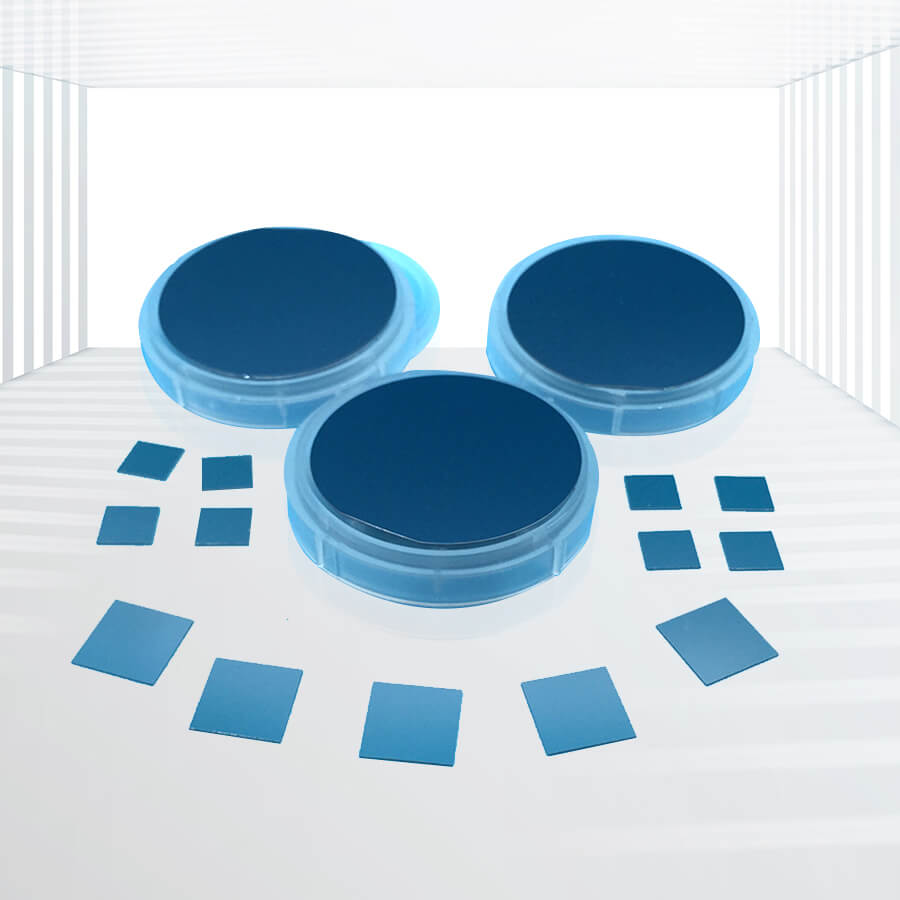
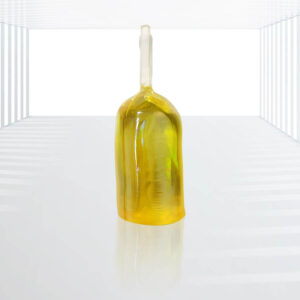
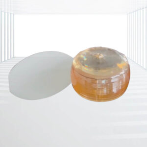
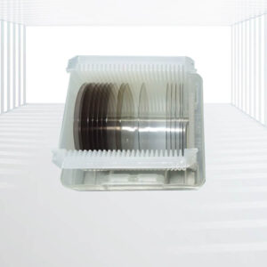
Indium Phosphide (InP) Wafers and Substrates
Direct Bandgap Material: Ideal for optoelectronic applications, enabling efficient optical transitions.
High Electron Mobility: Supports high-speed switching and high-frequency operation.
Scalable Sizes: Available in various diameters, including 2-inch, 3-inch, 4-inch, and 6-inch, to accommodate different manufacturing needs.
Strict Quality Control: Rigorous testing and inspection processes ensure defect-free wafers and substrates.
Applications: Laser Diodes, Photodetectors, High-Frequency Transistors, Integrated Circuits, Quantum Technologies, etc.
Kingwin Optics offers high-quality Indium Phosphide (InP) wafers and substrates, tailored to meet the demanding requirements of optoelectronic and electronic device manufacturing. Our InP wafers are grown using state-of-the-art techniques, ensuring consistent material quality and performance.
Specifications:
| Main performance parameters | |||||||
| Single crystal | adulterate | Conductive
type |
Carrier concentration
cm-3 |
Mobility (cm.)2/V.s) | Dislocation density (cm-2) | Standard substrates | |
| InP | Intrinsics |
N |
(0.4-2)*1016 | (3.5-4)*103 | 5*104 | Φ2×0.35mm
Φ3×0.35mm |
|
| InP | S | N | (0.8-3)*1018
(4-6)*1018 |
(2.0-2.4*103
(1.3-1.6*103 |
3*104
2*103 |
Φ2×0.35mm
Φ3×0.35mm |
|
| InP | Zn | P | (0.6-2)*1018 | 70-90
|
2*104
|
Φ2×0.35mm
Φ3×0.35mm |
|
| InP | Fe | N | 107-108 | ³2000 | 3*104 | Φ2×0.35mm
Φ3×0.35mm |
|
| Dimensions (mm) | Dia50.8×0.35mm, 10×10×0.35mm, 10×5×0.35mm can be customized according to customer needs | ||||||
| Surface roughness | Surface roughness (Ra): <=5A can provide atomic particle microscopy (AFM) inspection report |
||||||
| polished | Single-sided or double-sided | ||||||
| wrap | Class 100 clean bag, Class 1000 clean room | ||||||
| structure | Cube a=5.869 A | ||||||
| Crystal orientation | <100> | ||||||
| melting point oC | 1600 | ||||||
| Density g/cm3 | 4.79 | ||||||
| Bandgap width | 1.344 | ||||||
Key Features:
- Direct Bandgap Material: Ideal for optoelectronic applications, enabling efficient optical transitions.
- High Electron Mobility: Supports high-speed switching and high-frequency operation.
- Scalable Sizes: Available in various diameters, including 2-inch, 3-inch, 4-inch, and 6-inch, to accommodate different manufacturing needs.
- Strict Quality Control: Rigorous testing and inspection processes ensure defect-free wafers and substrates.
Applications:
- Laser Diodes: For high-speed data transmission in fiber-optic communication systems.
- Photodetectors: Essential in optical communication receivers and sensing applications.
- High-Frequency Transistors: In HEMTs and HBTs for microwave and millimeter-wave circuits.
- Integrated Circuits: For high-performance processing in data centers and advanced computing systems.
- Quantum Technologies: As a platform for quantum dot devices in emerging quantum computing and sensing.
Kingwin Optics offers customization options to suit specific customer requirements, including wafer orientation, doping levels, and surface treatments. Contact us for more information and to discuss your unique needs.


1.jpg)
2.jpg)
3.jpg)
晶体和晶圆1-300x300.jpg)
晶体和晶圆2-300x300.jpg)
陶瓷基板1-300x300.jpg)
陶瓷基板2-300x300.jpg)

3-300x300.jpg)

