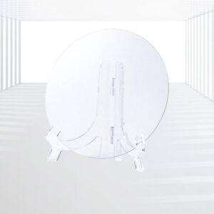
Nb:SrTiO3 Crystals and Substrates
Conductivity: The incorporation of niobium imparts conductivity to NSTO crystals, which is a significant advantage over undoped STO. This conductivity enables their use in electronic devices and thin film growth applications where electrical properties are crucial.
Structural Similarity to STO: NSTO crystals retain the excellent lattice match and physical properties of STO, making them ideal substrates for epitaxial growth of materials with Perovskite structures.
Customizable Doping Concentrations: NSTO crystals are available with various niobium doping concentrations, such as 0.05%, 0.1%, 0.5%, and 0.7%, allowing researchers and manufacturers to select the optimal doping level for their specific applications.
Versatile Film Growth Technologies: Similar to STO, NSTO substrates can accommodate diverse film growth technologies, including Magnet Sputtering, Pulsed Laser Deposition (PLD), Vaporization, MOCVD, CVD, and laser MBE.
Applications: Electronic Devices, Thin Film Growth Substrates, Optical Windows, Research and Development, etc.
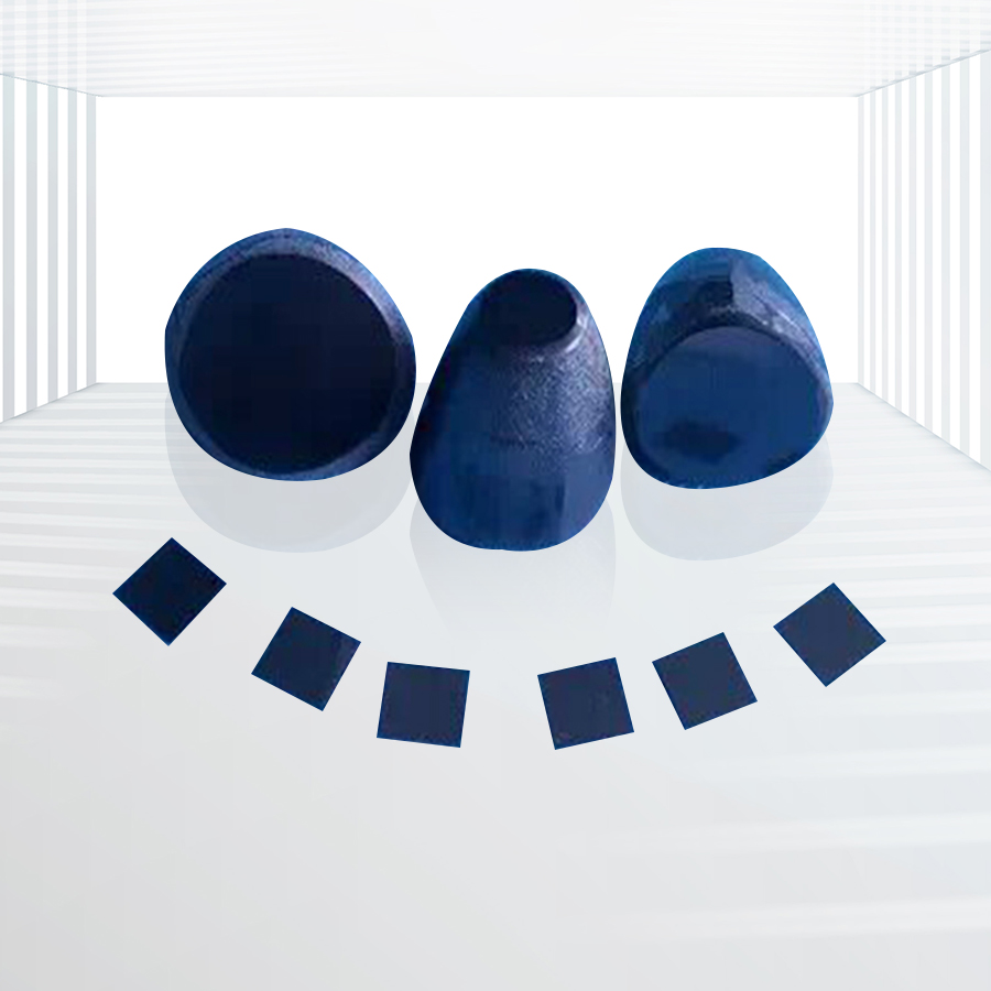
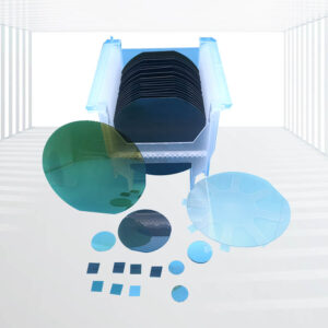
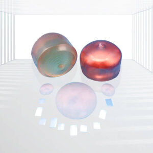
Nb:SrTiO3 (NSTO) crystals and substrates are modified versions of SrTiO3 (STO) with the addition of niobium (Nb) impurities. This doping results in the crystals acquiring conductive properties while maintaining the structural similarities of STO. NSTO crystals are widely used in various applications due to their unique combination of physical and electrical properties.
Specifications :
|
Main performance parameters |
||||
|
Nb: SrTiO3 level |
A |
B |
C |
D |
|
Nb concentration (wt%) |
1.0 |
0.7 |
0.5 |
0.1 |
|
Resistivity ohm-cm |
0.0035 |
0.0070 |
0.05 |
0.08 |
|
Mobility cm2/vs |
9.0 |
8.5 |
8.5 |
6.5 |
|
peculiarity |
Nb:SrTiO3 has a similar structure to SrTiO3 single crystals, but NSTO has electrical conductivity. The resistivity range varies between 0.1~0.001wt%. Conductive single-crystal substrates provide electrodes for thin films and devices. |
|||
|
size |
10×3,10×5,10×10,15×15,,20×15,20×20, |
|||
|
Ф15,Ф20,Ф1″, |
||||
|
thickness |
0.5mm,1.0mm |
|||
|
polished |
Single-sided or double-sided |
|||
|
Crystal orientation |
<100> <110> <111> |
|||
|
Plane orientation accuracy: |
±0.5° |
|||
|
Edge Orientation Accuracy: |
2° (up to 1° for special requirements) |
|||
|
Beveled wafers |
Wafers with edge-oriented crystal planes inclined at specific angles (1°-45°) can be processed according to specific needs |
|||
|
Ra: |
≤5Å (5µ m×5µ m) |
|||
|
wrap |
Class 100 clean bag, Class 1000 clean room |
|||
Advantages:
- Conductivity: The incorporation of niobium imparts conductivity to NSTO crystals, which is a significant advantage over undoped STO. This conductivity enables their use in electronic devices and thin film growth applications where electrical properties are crucial.
- Structural Similarity to STO: NSTO crystals retain the excellent lattice match and physical properties of STO, making them ideal substrates for epitaxial growth of materials with Perovskite structures.
- Customizable Doping Concentrations: NSTO crystals are available with various niobium doping concentrations, such as 0.05%, 0.1%, 0.5%, and 0.7%, allowing researchers and manufacturers to select the optimal doping level for their specific applications.
- Versatile Film Growth Technologies: Similar to STO, NSTO substrates can accommodate diverse film growth technologies, including Magnet Sputtering, Pulsed Laser Deposition (PLD), Vaporization, MOCVD, CVD, and laser MBE.
Applications:
- Electronic Devices: The conductivity of NSTO crystals makes them suitable for use in electronic devices, where they can serve as electrodes or substrates for thin film growth.
- Thin Film Growth Substrates: NSTO substrates provide an excellent lattice match for the epitaxial growth of high-temperature superconductors (HTSC) and various oxide thin films, enabling the production of high-quality films with optimal performance.
- Optical Windows: NSTO crystals can also be utilized for special optical windows, taking advantage of their transparency and structural stability.
- Research and Development: Due to their unique combination of properties, NSTO crystals are often used in research and development efforts to explore new materials and device concepts.
Kingwin Optics’ Nb:SrTiO3 (NSTO) crystals and substrates offer a unique combination of properties, making them ideal for a wide range of applications. With their conductivity, structural similarity to STO, customizable doping concentrations, and compatibility with diverse film growth technologies, NSTO crystals and substrates are valuable additions to any research or industrial setting.

.jpg)

1-300x300.jpg)
