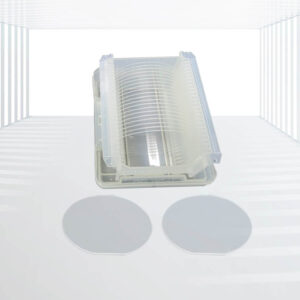
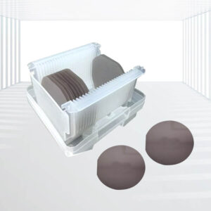
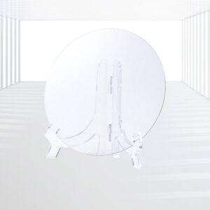
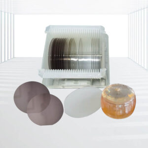
Sapphire (Al2O3) Substrates and Wafers
Versatility: Sapphire Wafers and Substrates are suitable for a wide range of applications, including III-V and II-VI compound thin film growth for semiconductors, Light Emitting Diodes (LEDs), high-temperature superconducting (HTSC) thin films, Microelectronic ICs (Silicon on Sapphire Integrated Circuit, SOS), Hybrid Microelectronic applications, and ferromagnetic/ferroelectric thin film growth.
Uniform Dielectric Constants: A-plane Sapphire Substrates and Wafers offer uniform dielectric constants and high electrical insulation, making them suitable alternatives for Hybrid Microelectronic applications, including HIC and MCM.
High-Speed Silicon On Sapphire (SOS): R-plane Sapphire Substrates and Wafers are ideal for the hetero-epitaxial deposition of silicon for Microelectronic ICs, enabling high-speed performance.
MOCVD Growth: C-plane Sapphire Substrates and Wafers are mainstream options for Metal Organic Chemical Vapor Deposition (MOCVD) growth of a series of III-V and II-VI compound thin films, including GaN, AlN, AlGaN, and InGaN, used in manufacturing blue, violet, and white light-emitting diodes (LEDs) and blue laser diodes (LDs).
Ferroelectric Thin Film Growth: C-plane Sapphire Substrates and Wafers are also suitable for the growth of ferroelectric thin films, such as (Pb, La)(Zr, Ti)O3 (PLZT), making them candidates for manufacturing new functional electronics.
Ferromagnetic Thin Film Growth: M-Plane Sapphire Substrates and Wafers are competent in the ferromagnetic thin film growth of Mn1−xS and other materials, making them suitable for applications such as solar-blind ultraviolet detection.
Applications: Semiconductors, Light Emitting Diodes (LEDs), High-Temperature Superconductors, Microelectronic ICs, Hybrid Microelectronic Applications, Functional Electronics, etc.
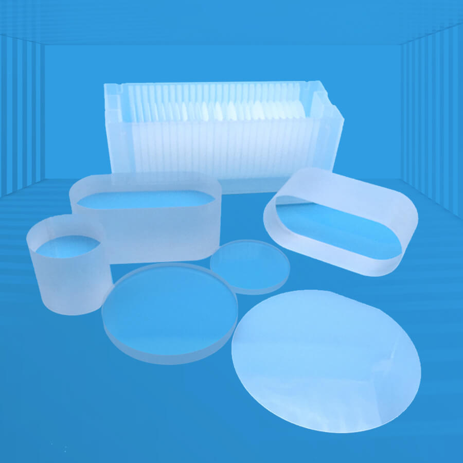
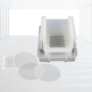
Kingwin Optics is pleased to present our Sapphire Wafers and Substrates, recognized for their exceptional high-temperature resistance, chemical corrosion resistance, electrical insulation, wide optical transmission, and unrivaled mechanical hardness and wear resistance. Sapphire’s strong molecular bonding enables the production of thinner pieces without fracture, making it an ideal substrate material for the epitaxial growth of various thin films.
Specifications:
| Main performance parameters | |||
| crystal system | Hexagonal crystal system | ||
| Unit cell constant | a=4.748Å c=12.97Å | ||
| density | 3.98(g/cm3) | ||
| melting point | 2040℃ | ||
| Mohs hardness | 9 | ||
| Coefficient of thermal expansion | 7.5 (x10-6/ oC) | ||
| Thermal conductivity (kcal/degree cm sec) | ⊥c | //c | |
| 23℃ | 0.055 | 26℃ 0.060 | |
| 77℃ | 0.040 | 70℃ 0.041 | |
| Dielectric constant | ~ 9.4 @300K at A axis ~ 11.58@ 300K at C axis | ||
| Crystal orientation | A-plane | <11-20> | 2.379A |
| R-plane | <1-102> | 1.740A | |
| M-plane | <10-10> | 1.375A | |
| C-plane | <0001> | 2.165A | |
| Crystal tolerancy | ±0.5° | ||
| Conventional dimensions and tolerances | 10×3,10×5,10×10,15×15,20×15,20×20, | ||
| Conventional thicknesses and tolerances | 0.5mm,1.0mm | ||
| polished | Single-sided or double-sided | ||
| Surface roughness | Ra<5Å(5×5μm) | ||
| wrap | Class 100 clean bag, Class 1000 clean room | ||
Key Advantages:
- Versatility: Sapphire Wafers and Substrates are suitable for a wide range of applications, including III-V and II-VI compound thin film growth for semiconductors, Light Emitting Diodes (LEDs), high-temperature superconducting (HTSC) thin films, Microelectronic ICs (Silicon on Sapphire Integrated Circuit, SOS), Hybrid Microelectronic applications, and ferromagnetic/ferroelectric thin film growth.
- Uniform Dielectric Constants: A-plane Sapphire Substrates and Wafers offer uniform dielectric constants and high electrical insulation, making them suitable alternatives for Hybrid Microelectronic applications, including HIC and MCM.
- High-Speed Silicon On Sapphire (SOS): R-plane Sapphire Substrates and Wafers are ideal for the hetero-epitaxial deposition of silicon for Microelectronic ICs, enabling high-speed performance.
- MOCVD Growth: C-plane Sapphire Substrates and Wafers are mainstream options for Metal Organic Chemical Vapor Deposition (MOCVD) growth of a series of III-V and II-VI compound thin films, including GaN, AlN, AlGaN, and InGaN, used in manufacturing blue, violet, and white light-emitting diodes (LEDs) and blue laser diodes (LDs).
- Ferroelectric Thin Film Growth: C-plane Sapphire Substrates and Wafers are also suitable for the growth of ferroelectric thin films, such as (Pb, La)(Zr, Ti)O3 (PLZT), making them candidates for manufacturing new functional electronics.
- Ferromagnetic Thin Film Growth: M-Plane Sapphire Substrates and Wafers are competent in the ferromagnetic thin film growth of Mn1−xS and other materials, making them suitable for applications such as solar-blind ultraviolet detection.
Applications:
- Semiconductors: Sapphire Wafers and Substrates are used for the growth of III-V and II-VI compound thin films in semiconductor manufacturing.
- Light Emitting Diodes (LEDs): Sapphire is a preferred substrate material for the production of blue, violet, and white LEDs due to its excellent optical and thermal properties.
- High-Temperature Superconductors: Sapphire Wafers and Substrates are used for the growth of high-temperature superconducting thin films, such as Y-series and La-series materials.
- Microelectronic ICs: Sapphire is used as a substrate material for Silicon on Sapphire Integrated Circuits (SOS), providing high-speed performance and electrical insulation.
- Hybrid Microelectronic Applications: Sapphire Wafers and Substrates are used in Hybrid Integrated Circuits (HIC) and Multi-Chip Modules (MCM) due to their uniform dielectric constants and high electrical insulation.
- Functional Electronics: Sapphire is used for the growth of ferroelectric thin films, such as PLZT, enabling the manufacture of new functional electronics.
Kingwin Optics’ Sapphire Wafers and Substrates offer exceptional properties and versatility for various applications in the fields of semiconductors, optics, and microelectronics. With our commitment to quality and precision, trust Kingwin Optics for all your Sapphire Wafer and Substrate needs.

3.jpg)
-.jpg)
1.jpg)
2.jpg)
4.jpg)
5.jpg)
6.jpg)
3-300x300.jpg)
